Control of light polarisation inside light-emitting diodes and semiconductor lasers for broadband communication
The laser-based optical communications technique is one of the solutions that are contemplated to significantly increase the bit rate in comparison to radio conections due to the high frequency of the signal and the low divergence of the laser-emitted optical beam. Information transmission between a satellite and the Earth could be increased by two orders of magnitude. Modern technological devices rely on light intensity modulation to transmit information, which presents limitations regarding speed and energy consumption. We are developing a method based on the modulation of light polarisation, allowing for a higher speed, up to 1 THz. In addition, this concept is less energy-consuming since the light intensity remains constant, regardless of the speed at which we modulate polarisation. This principle consists in adding a magnetic layer to a diode capable of selecting the spin of the electrons. This spin selection allows to control the polarisation of photons emitted by the light-emitting diode. Using the spin Hall effect, we demonstrated that it is possible to control the polarisation of light by electrical spin injection, enabling to transmit data at a high speed.

Diagram of the spin LED structure with an active layer composed of InAs nanocrystals. The spin injector is a structure composed of MgO (2.5 nm)/CoFeB (1.2 nm)/Ta (3 nm)/Cr (3 nm). The microscopy image is obtained with the high-resolution light-field mode and shows the multi-layered structure of the injector.
Control of light-matter interaction at the nanometric scale with optical nanoantennas
Optical nanoantennas allow to gather around them intense and confined electromagnetic fields that can be used to control light-matter interactions at the nanometric scale. For instance, we can use them to reinforce the fluorescence emission of quantum emitters, to detect nearby molecules or to trigger photochemical reactions. We are working on designing and manufacturing plasmonic and dielectric nanoantennas, on functionalisation techniques to graft molecules onto nanostructures as well as on experimental techniques to characterise the optical response from resulting hybrid systems (extinction coefficient and photoluminescence measurements, Fourier plane imaging, near-field imaging, ellipsometry). The materials can be prepared by electron-beam or optical lithography, sol-gel deposition, or under ultra-high vacuum with MBE techniques. Diverse metals as well as highly-doped semiconductors are used, enabling to cover a range of wavelengths from ultraviolet to mid-infrared.

Manifestation in a transmission electron microscope of multiple resonance phenomena within an aluminum-based fractal structure. (A) HAADF image of the fractal structure, (B) and (C) obtained spectrometry images of electron energy loss indicating different resonant modes.
Exploring and enhancing the light emission properties of semiconductor nanocrystals in colloidal suspension
Semiconductor nanocrystals present remarkable optical properties which differ from those of bulk materials due to their nanometric size. Among those properties, they offer wide absorption bands, emission of light adjustable in energy depending on the size and composition, high luminosity and photostability). We synthesise a wide variety of such nanocrystals by colloidal way, based on non-toxic elements by optimising their properties in aqueous solution. Its intended applications include pollutant sensors, optical and bimodal imaging and lighting devices.

Creation of semiconductor nanocrystals (Ag-In-Ga-Zn-S alloy) doped with transition metals using the colloidal method. The optical and magnetic properties induced by the manganese doping of these materials enable their utilisation for bimodal optical and magnetic imaging.
Hybrid organic-inorganic perovskites for broadband emission or light polarisation control
Hybrid halide perovskites (HPP) are innovative materials composed of an inorganic structure which contains organic cations. These materials possess interesting semiconducting properties such as the absorption or emission of photons. Chemical composition engineering makes it possible, when substituting central metal (Pb, Sn, Ge) or halogen (Cl, Br, I), to adjust physical properties such as the electronic gap and, as a result, change the wavelength of the absorbed or emitted photons. This ability to modulate the wavelength of the emitted light contributes to making these HPPs promising materials for applications in optoelectronics.
On the one hand, we develop perovskites that are able to emit light on a very wide spectral range (“white” light emission) and on the other hand, we create perovskites that are able to emit controlled light with polarisation. The latter property is obtained by intentionally inserting a chiral cation into the structure. The cation enforces a crack in the inversion symmetry and can transfer its chirality to the inorganic semiconducting structure. This mechanism allows for the spin control of the injected charge carriers (electrons and holes) whose recombination induces the emission of a right-hand or left-hand circularly polarised light depending on the spin of the charge carriers. Applications in telecommunications are being considered.

White light emission inside the 2D hybrid perovskite (C6H11NH3)2CdBr4 resulting from the confinement of charge carriers in inorganic 2D layers.
Ultrafast laser processes on dielectric mediums and innovative semiconductors, applications in photovoltaic technology and sensors
The energy, technological and digital challenges of our times lead us to broaden the physics of semiconductors to consider new materials, processes and devices. Amongst others, those challenges relate to new approaches allowing the optimal exploitation of photovoltaic energy, the conception of new sensors, and the use of technologies based on abundant materials with a sustainable life cycle. We are working on the physics of semiconductors, organic and inorganic alike. Our research activities mainly focus on the growth or deposit of nanostructured thin layers of materials, the modification of materials with physical or chemical treatments, the study of optoelectronic properties which significantly impacts the functioning of components and on the possible microstructuring or welding processes of materials using an ultrashort pulse laser.

Glass sample welded by femtosecond laser pulses using a focalisation device with long focal length.
Photorefractive materials
A photorefractive material is a type of optical material that is capable of altering its refractive index in response to its exposition to intense, commonly coherent light (that of a laser for instance). This property is due to internal mechanisms such as the trapping and movement of charge carriers, followed by the redistribution of charges into the material.
More specifically, the illumination of the material by an intense laser generates charges which move under the effect of a light intensity gradient. Charges that are trapped in the material form an intense electric field which modifies the refractive index (Pockels effect), allowing for the modification of the light propagation and creation of photo-induced waveguides for instance.
We examine the optical properties of various photorefractive materials for different doping natures and densities, allowing for visible until near-infrared wavelengths to benefit from this photorefractive effect . We utilise this photorefractive property to create optical waveguides that are reconfigurable inside matter. The use of semiconductor photorefractive materials allows to significantly decrease the time constant of these light-matter interactions.

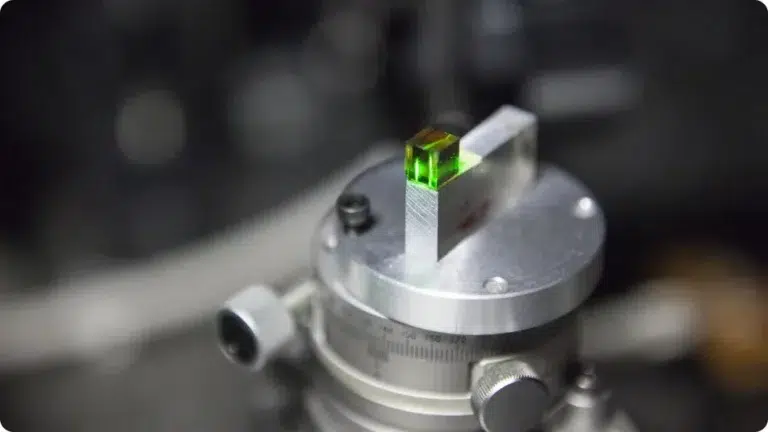
Interaction of light in a photorefractive crystal.
LCP-A2MC laboratory (Laboratoire de Chimie et Physique – Approche Multi-échelles des Milieux Complexes), Université de Lorraine
Sol-gel synthesis, modeling
L2n (Light, Nanomaterials, Nanotechnologies) University of Technologies of Troyes
Nanotechnologies, light-matter interaction at the nanometric scale
Photo-induced waveguides, optical patterns, non-conventional beams interaction and neuro-inspired computing, photorefractive materials
CRM2 laboratory (Cristallographie, Résonance Magnétique et Modélisations), Université de Lorraine
Hybrid perovskites
Institut Jean Lamour, Université de Lorraine
MBE synthesis, infrared plasmonics
UMR 7274 (Laboratoire Réactions et Génie des Procédés) laboratory, Université de Lorraine
Quantum dots, colloidal synthesis
Photorefractive materials, photo-induced waveguides, slowing of light, solitons and spatial patterns
Photorefractive materials, photo-induced waveguides, slowing of light, solitons and spatial patterns